Atom-to-Circuit modeling tool to estimate the performance of 2D materials
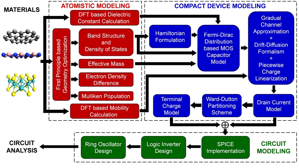
Functionality of an electronic device originates from the interfacial properties of its constituent materials. Advancement of nanofabrication technology has opened up the possibility of realizing interfaces at their ultimate-limit by vertical stacking or parallel stitching of 2D materials. Since these new materials inherit diverse electronic properties, novel device functionalities could be engineered from such atomically thin interfaces. In semiconductor industry, however the process integration for any new material has always been a capital and time intensive affair.It is also a difficult task to select appropriate 2D materials from the plethora without assessing their performance at circuit level. Thus, a modeling framework, that enables systematic performance evaluation of new materials at device and circuit levels before entering into capital-intensive manufacturing phase, is in great demand. Such models must be first principles based so that the assessment could be conducted at the early phase of technology research even before the wafer is available. Despite significant efforts on synthesis and fabrication, community lacks such modeling framework, which can predict integrated circuit performance solely from the crystallographic information of the constituent transistor materials.
In this view, we propose an ‘atom-to-circuit’ modeling framework for all-2D MISFET (Metal-Insulator-Semiconductor Field-Effect Transistor), which has recently been conceived by vertically stacking of semiconducting transition metal dichalcogenide (e.g. MoS2), insulating hexagonal boron nitride and semi-metallic graphene. In a multi-scale modeling approach, we start with the development of first principles based atomistic model for such system to study the fundamental electronic properties and charge transfer at atomic level. The energy band-structure thus obtained is then used to develop purely physics based compact device model to assess the transistor characteristics. Finally, those models are implemented in professional circuit simulator to facilitate design and simulation of integrated circuits. Since the proposed modeling framework translates atomic level phenomena (e.g. band-gap opening in graphene) to a circuit performance metric (e.g. frequency of a ring oscillator), it may provide solution to the design-technology co-optimization challenges for any new material. It bridges between first-principle based material modeling tools and industry standard circuit simulators and facilitates seamless design flow from 2D materials to integrated circuits.

- Biswapriyo Das and Santanu Mahapatra, “An Atom-to-Circuit modeling approach to all-2D Metal-Insulator Semiconductor Field-Effect Transistors” npj 2D Materials and Applications, Nature publication group, 2018, DOI:10.1038/s41699-018-0073-3
- Code: https://osf.io/me236/
- Group: http://nsdrl.dese.iisc.ac.in
- YouTube Channel: nsdrlTube


