MXene transistor with intrinsically low resistive contacts
When physicists Walter Brattain and John Bardeen first demonstrated the point-contact transistor at Bell Laboratories 75 years ago, no one could have predicted how their discovery would change the course of human history. Without the transistor, we would not be living in the world we know today.
What started out as a point-contact three terminal semiconductor device has evolved over time both in terms of its current control mechanism (from bipolar junction transistor to various forms of field effect transistors) and size (sub-millimeter to deca-nanometer). Downscaling like this, aided by the astounding sophistication of semiconductor technology, has allowed us to pack millions of transistors within a unit area of silicon wafer, enabling us to run even advanced machine learning platforms such as TensorFlow on an Android phone.
However, such downscaling has pushed silicon technology to its limit and semiconductor industry has been forced to look for other alternatives. After the discovery of graphene in 2004, various atomically thin layered materials (also known as 2D materials) have attracted attention for transistor applications. Because of their inherent “thin-ness” they promise to outperform bulk silicon in technology scaling.
 After the first revelation of monolayer molybdenum disulphide (MOS2)-based metal-oxide-field-effect transistors in 2011, integrated circuits built upon 2D transistors have been demonstrated for diverse applications: simple logic inverter,1-bit microprocessor, operational amplifier, and neuromorphic computation. Despite such intense efforts, the high contact resistance at the interface between the 2D material and the external metallic circuits has appeared as the key obstacle for realising high-performance transistors with sub-decananometer channel lengths.
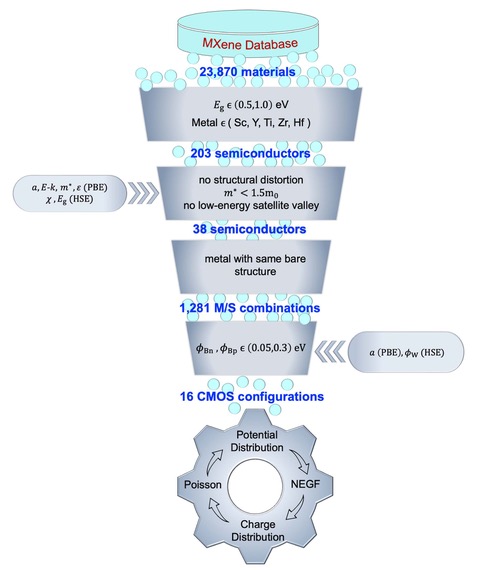
Even though dozens of 2D materials have been explored experimentally (and hundreds of them computationally), MXenes have been overlooked for MOS transistor applications. MXenes are a group of non-Van der Waals 2D materials first reported in 2011, has gathered attention due to their fascinating mechanical and electronic properties. In new work, researchers at the Department of Electronic Systems Engineering, IISc show how MXene’s rich chemistry can be used to create doping-free 2D transistors with intrinsically low resistive contacts while maintaining balance mode operation.
To validate their concept, they have developed a high-throughput computational pipeline to identify 16 such CMOS configurations by screening materials from a large MXene database (hosting more than 23,000 materials) and then predicting their performance with an in-house GPU-based quantum transport simulator. Performance of these devices has been found to meet the requirements of the international roadmap for devices and systems (IRDS) for several benchmark metrics. The proposed balanced-mode, functional-engineered MXene transistors may lead to a realistic solution for the sub-decananometer technology scaling by enabling doping-free intrinsically low contact resistance.
REFERENCE:
Guha S, Kabiraj A, Mahapatra S, High-throughput design of functional-engineered MXene transistors with low-resistive contacts, npj Computational Materials (2022).
https://doi.org/10.1038/s41524-022-00885-6
LAB WEBSITE:
https://labs.dese.iisc.ac.in/nsdrl/