Pushing the transistor reliability and operating limits for efficient FinFET SoC Integration
Nano electronic devices is an area which is responsible for sweeping out the bulkiness of electronic products and thereby aiding the exponential down-scaling of technology. This is achieved by improved non-planar transistor device designs like FinFETs. Fin Field Effect transistors (or FinFETs) are the newer technology options, which possess the unique capability of current conduction in different orientation, hence encouraging further scaling of these transistors. In FinFETs, the channel is risen above the level of the insulator which gives it the shape of a fin, hence the name FinFET. This fin-shaped gate electrode is responsible for excellent electrostatic control over the channel, and provides lower leakage and higher drive currents, which makes FinFETs as the most promising candidates for ultra large scale integration.
 However, integrating high voltage functionalities in FinFET nodes for System on Chip (SoC) is still a major technological concern. Making the FinFET devices to work in a narrow operating window or working at smaller voltages is less challenging than making them work under extended conditions with various reliability threats or operating them at higher voltages. In an SoC, low voltage modules like memory, logic and other computational blocks can be implemented using sub-1V FinFET transistors. However, to interface the chips with the external world, special voltage classes of Input/Output (I/O) devices (typically 1.8V or 3.3V) are required. For the design of power management modules, high voltage FinFETs or LDMOS-Fins (typically 5V or 10V) are employed. In addition to this, robust functional devices and special Electrostatic Discharge (ESD) protection devices are needed for SoC integration. Insight into the physics of various device reliability challenges and high voltage operation is imperative to develop highly rugged devices.
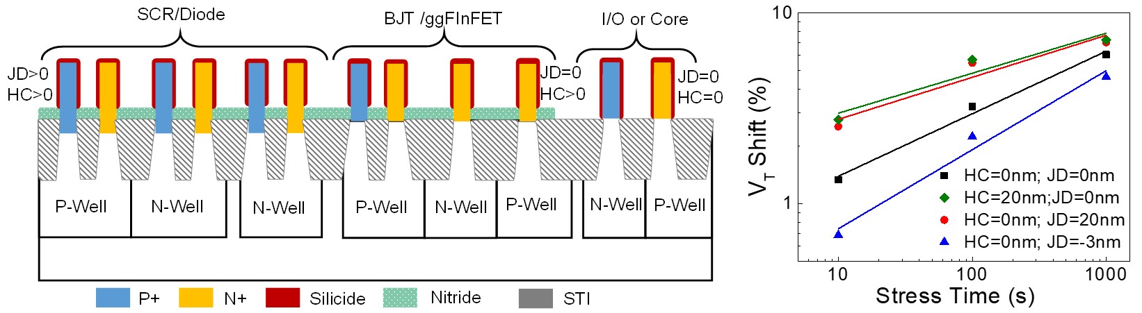
 This work enabled the researchers to understand the mechanisms behind ESD, Latch-Up and Hot Carrier reliability in FinFET devices, which allowed to invent special ESD protection techniques and high voltage concepts enhancing the reliability limits of FinFET technology. Through appropriate contact and junction profile engineering, the team was able to boost the ESD robustness of FinFETs by 6X, however, it was found to adversely affect the long term reliability of the functional devices. This lead to the proposition of a hybrid contact and junction engineered scheme, wherein, different device types on the chip are employed with unique contact/junction profiles depending upon their application. This selective contact/junction profile engineering enabled to achieve ESD robust protection devices as well as reliable core functional devices in FinFET technology.
References:
researchmatters.in/news/iisc-research-pushes-reliability-and-operating-limits-ultra-dense-finfet-system-chips
http://mayank.dese.iisc.ac.in
Website URL: http://mayank.dese.iisc.ac.in/
http://msdlab.dese.iisc.ac.in/


