Fully-printed circuits on PET plastics
A study by Allied market research group predicts that the flexible and wearable electronics market will exceed USD 42 billion by 2027. Besides conductive inks and a wide variety of sensors, the recently emerging device participants in printed electronics are flexible displays, circuits, flexible memory, energy conversion and storage devices. Notably, control electronics is essential for all these applications and a three-terminal device called field-effect transistor (FET) is the building block which comprises all the electronic circuits. Solution-processed/printed FETs have traditionally been fabricated using organic semiconductors. Recently, inorganic, especially oxide semiconductors are also being used to realise high mobility/high performance transistors and circuits. However, one of the fundamental drawbacks is the high process temperature of oxides, thereby limiting the choice of inexpensive substrates. Next, the lack of high-quality hole conducting (p-type) oxide semiconductors and the inherent lack of mechanical strain tolerance of ceramic oxides also limit their flexible electronic applications.
In this regard, researchers from the Department of Materials Engineering led by Subho Dasgupta, Associate Professor, proposed and demonstrated a device geometry (coined as edge-FET architecture), where a semiconductor layer is sandwiched between two metal layers, resulting in near vertical electronic transport. The narrow channel devices thus produced allow the use of printed oxide semiconductor nanoparticles to comprise the transistor channel. This removes a high temperature annealing step and reduces the process temperature to ~100 °C, low enough for PET or paper substrates, without compromising on the transistor performance. The absence of high-quality p-type semiconductor has been addressed with pseudo-CMOS circuit design, and interestingly a very high signal gain >200 has been recorded at a supply voltage of only 2 V, alongside an operation frequency >300 kHz. Further, the use of semiconductor nanoparticles and the vertical device architecture also results in mechanical reliability as the electronic transport remains unaltered even for minor cracks in the semiconductor layer; consequently, a tensile strain tolerance up to 5% can be demonstrated.
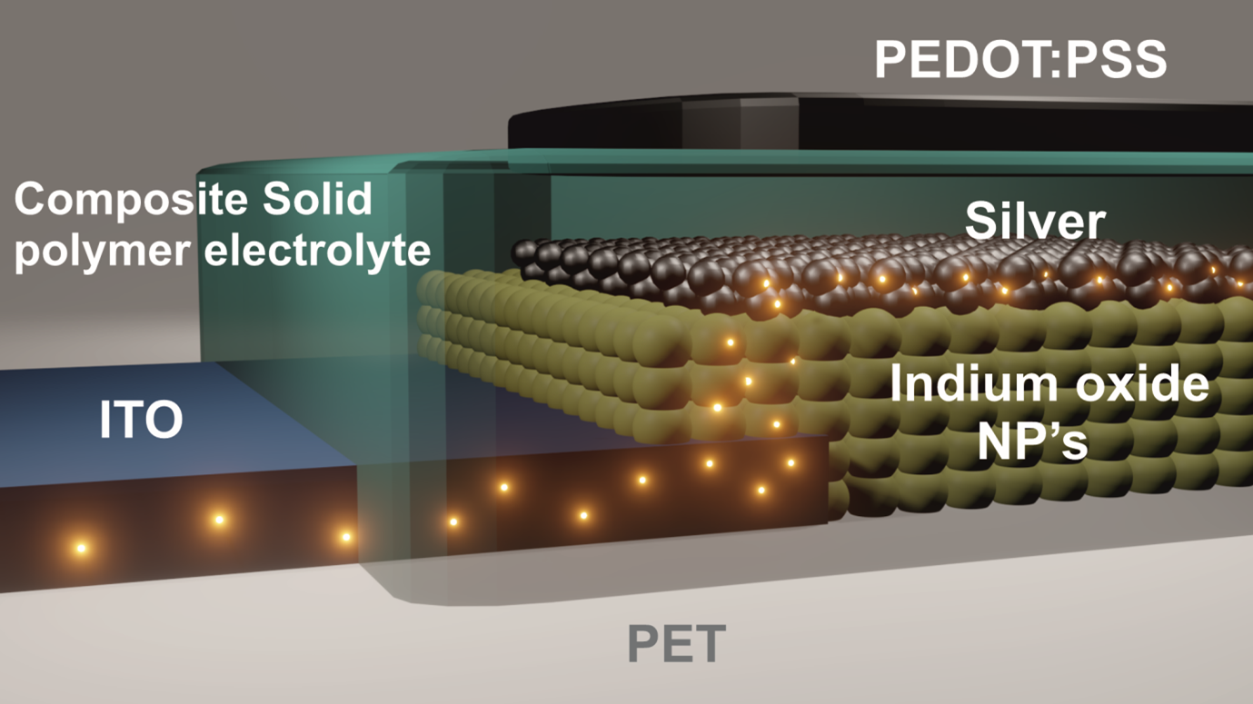
Schematic representation of In2O3 nanoparticle channel thin film transistor (TFT) with edge-FET architecture printed on PET substrate
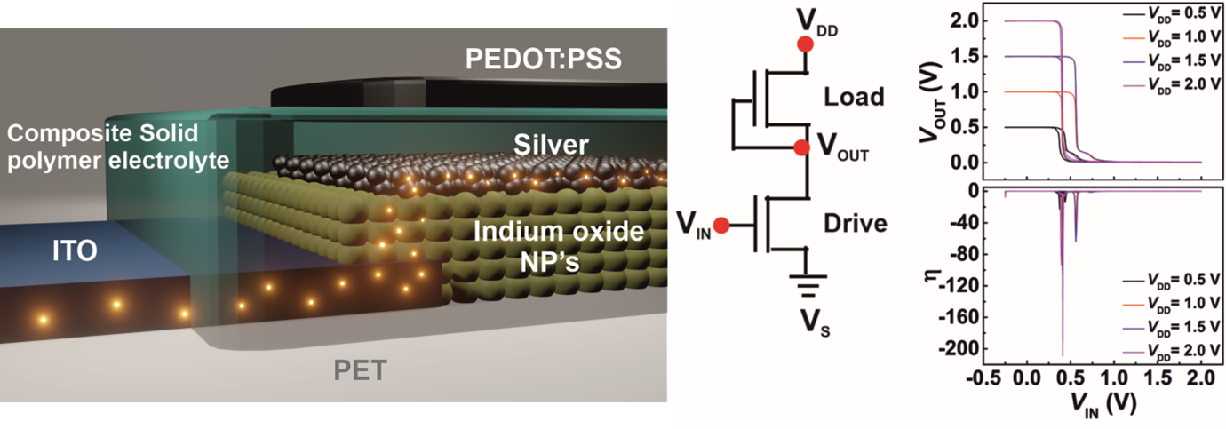
(From left to right) Schematic representation of indium oxide nanoparticle channel TFTs with edge-FET device architecture, schematic of depletion load-type, pseudo-CMOS inverter, voltage transfer characteristics (VTC) and corresponding gain of a fully printed indium oxide nanoparticle channel pseudo-CMOS inverter on PET substrate.
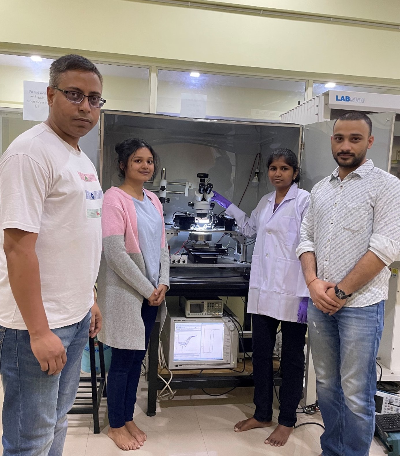
(From right to left Jyoti Ranjan Pradhan, Divya Mitta, Sushree Sangita Priyadarsini, Subho Dasgupta)
Reference:
Divya, Mitta, Jyoti Ranjan Pradhan, Sushree Sangita Priyadarsini, and Subho Dasgupta. “High Operation Frequency and Strain Tolerance of Fully Printed Oxide Thin Film Transistors and Circuits on PET Substrates.” Small (2022): 2202891.
https://onlinelibrary.wiley.com/doi/full/10.1002/smll.202202891
Group Website: https://materials.iisc.ac.in/~dasgupta/index.html


