Electronics at the atomic limit: a multi-functional van der Waals tunnel diode
With the ever-increasing demand for higher density and more functionalities in electronic chips, nano-electronic devices are highly promising owing to the exotic features they offer. Electronic devices derived from low dimensional systems offer new pathways to achieve unparalleled performance scores and are excellent candidates for beyond silicon technologies.
Esaki (tunnel) diode is a nonlinear device which exhibits a negative correlation between the current flowing though it and the voltage driving the current. Its discovery in the year 1957 has been a historic landmark for the semiconductor industry and since then Esaki diodes has remained as a key element in electronic circuits.
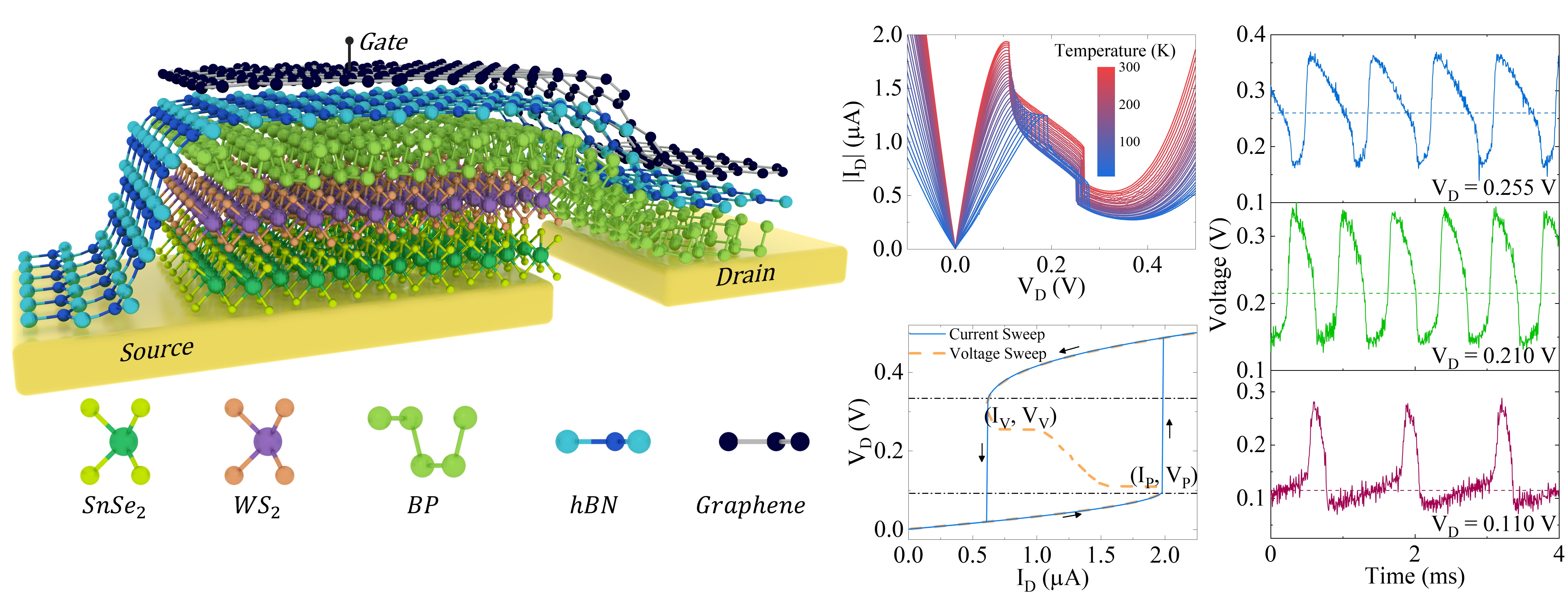
In a recent study, researchers from the Quantum Electronics Laboratory of the Department of Electrical Communication Engineering have designed and experimentally demonstrated a highly versatile vertical tunnel diode, where the active layer is made of few tens of nanometre thick layered materials. They were able to thin down the depletion region of the diode to a thickness of ~7 Å by introducing an artificial monolayer depletion region. Using different biasing constraints, they were able to transform the tunnel diode into a voltage controllable reactive-element-free oscillator or an ultra-low-power single element memory cell. The reactive-element-free nature of the oscillator makes it easily integrable on chip and the ultra-low-power consumption of the memory cell is ideal for low power electronics. The memory cell also features a low footprint important for high density memory applications. The proposed tunnel diode retains its versatile operation at low temperatures (-270◦C) making it suitable for cryogenic electronics as well.
I
The architecture of the tunnel diode is shown in the left panel. The nonlinear DC response of the system at temperatures ranging from ambient to cryogenic, operation as a single-element memory cell, and its operation as a reactive-element-less voltage-controlled oscillator are given in the right panel.
Reference
N. Abraham, K. Murali, K. Watanbe, T. Taniguchi, and K. Majumdar, Astability versus Bistability in van der Waals Tunnel Diode for Voltage Controlled Oscillator and Memory Applications, ACS Nano, 2020, DOI:10.1021/acsnano.0c06630.
Lab Website
https://ece.iisc.ac.in/~kausikm/
Photo Credits : Kausik Majumdar Lab


