10 February 2026
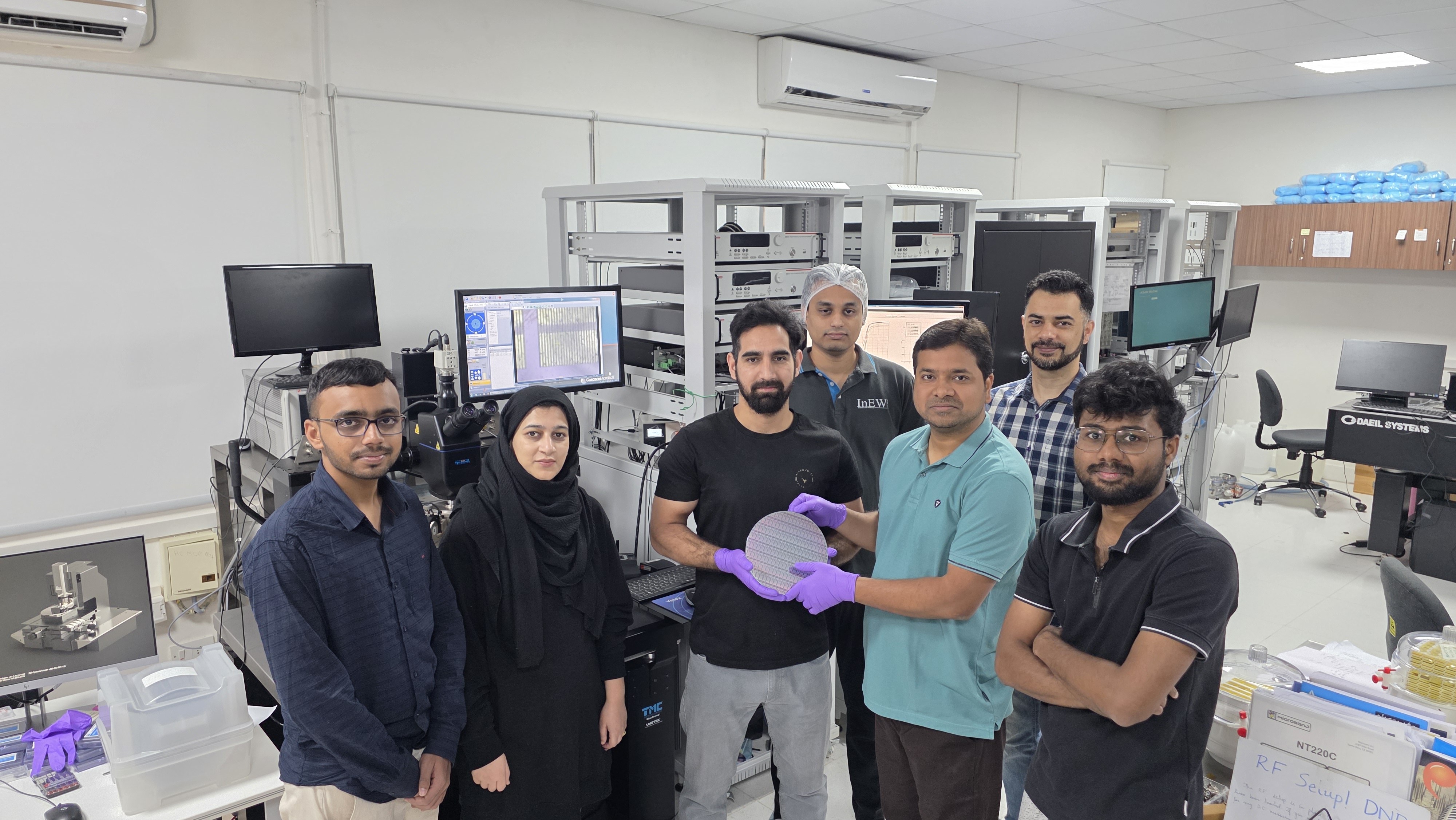
Mayank Shrivastava (third from right) holding a representative power device 8” wafer, with some of his PhD students who work on various aspects of GaN Power and RF technology, in ESE, IISc (Credit: Mayank Shrivastava)
Researchers at the Indian Institute of Science (IISc) have uncovered fundamental insights into designing gallium nitride (GaN) power transistors, making them safer and easier to utilise in high-value electronics such as electric vehicles and data centres.
GaN can reduce energy losses significantly and cut down the size of power converters and other power electronics modules by three times, but adoption has been slow owing to the limited capability of its gate, which controls the flow of current. With currently used commercial transistors that use a p-GaN gate, the device starts conducting at a low threshold voltage (the gate voltage needed to switch it on), which is typically around 1.5–2 V. Such transistors also start to leak current above 5-6V.
What has been missing so far is a fundamental understanding of how these transistors are controlled by their gate and what factors determine the threshold voltage. Researchers at the Department of Electronic Systems Engineering (ESE), IISc, carried out a two-part study to investigate these phenomena.
“What is unique here is the two-step approach: we first established the missing physics link between p GaN depletion state, leakage pathways, and turning on, and then used that understanding to engineer a new gate stack that delivers a much more ‘MOSFET-like’ gate behaviour,” says Mayank Shrivastava, Professor and Chair at ESE and corresponding author of the studies.
In the first part, the IISc team designed several new gate variants and connected electronic measurements to models and microscopy. They showed that the device behaviour depends on whether the p-GaN layer is fully or partially depleted. When partially depleted, tiny leakage paths decide the outcome – if positive charge accumulates at a critical interface, the device turns on early; if that accumulation is suppressed, depletion extends first and the transistor turns on later, at a higher threshold. “It was surprising how strongly ‘small’ leakage paths can decide the entire turn-on behaviour,” says Shrivastava.
Using these insights, the team designed and demonstrated new metal-based gate stacks that can cut gate leakage by up to 10,000 times, while improving threshold stability and reaching gate breakdown voltages up to ~15.5 V.
In the second part, they translated these fundamental insights into an integrated AlTiO (aluminium–titanium oxide)-based p-GaN gate stack – a completely new and patented proposal that suppresses unwanted charge injection and forces the high-threshold depletion-extension mode. The resulting devices reach an ultrahigh threshold voltage of >4 V – close to silicon-powered MOSFET levels – while maintaining strong gate control, improving threshold stability, and demonstrating an ultra-high gate breakdown voltage. “This can speed up GaN adoption in EV power converters, server or data centre power supplies, renewable energy inverters, and other high-reliability, high-power switching applications,” says Rasik Rashid Malik, PhD student at ESE and lead author.
Such advancements can boost the deployment of GaN technology in applications where reliability, robustness, and performance margins are paramount, opening up indigenous opportunities to leapfrog in providing advanced electronic solutions.
The team now seeks to scale this technology for commercial deployment through a combination of government support, industry licensing, and collaborative partnerships.
“Achieving a higher threshold voltage together with low leakage and robust gate overdrive margin is one of the key enablers for GaN’s next phase of adoption,” says Shrivastava. “That is exactly what we set out to solve.”
REFERENCES:
Malik RR, Joshi V, Chaudhuri RR, Thakare AV, Shrivastava M, Achieving ultrahigh threshold voltage in enhancement-mode AlGaN/GaN HEMTs with an AlxTiyO/p-GaN integrated gate stack—Part II, IEEE Transactions on Electron Devices (2026)
https://ieeexplore.ieee.org/document/11359444
Malik RR, Chaudhuri RR, Joshi V, Karthik SR, Shrivastava M, Physical insights into turn-on mechanisms in p-GaN gate AlGaN/GaN HEMTs—Part I, IEEE Transactions on Electron Devices (2025)
https://ieeexplore.ieee.org/document/11219199
These works are funded by the Advanced Manufacturing Technology programme, DST. Initial part of this work was funded by a Core Research Grant of SERB/ANRF.
CONTACT:
Mayank Shrivastava
Professor & Chair
Department of Electronic Systems Engineering (ESE)
Indian Institute of Science (IISc)
E-mail: mayank@iisc.ac.in
Phone: +91-80-2293-2732
Website: http://mayank.dese.iisc.ac.in/
NOTE TO JOURNALISTS:
a) If any of the text in this release is reproduced verbatim, please credit the IISc press release.
b) For any queries about IISc press releases, please write to news@iisc.ac.in or pro@iisc.ac.in.
