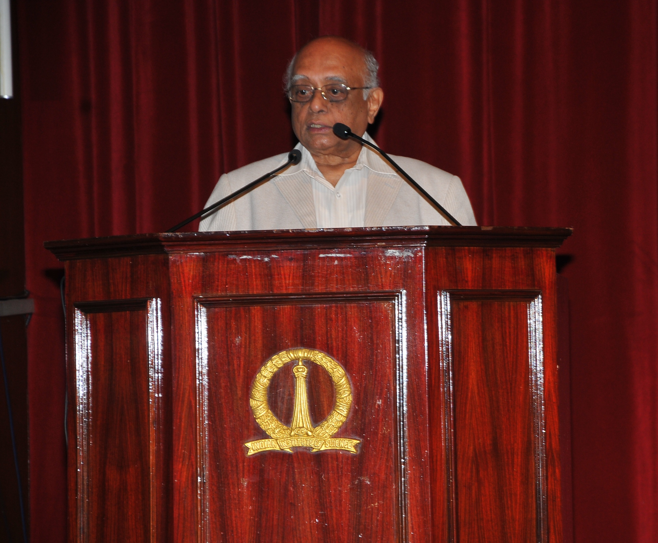
We are deeply saddened by the passing of Dr R Chidambaram, a distinguished alumnus of IISc, on 4 January 2025. One of India’s outstanding scientific leaders, he was the former Chair of the Atomic Energy Commission and former Principal Scientific Adviser, and made key contributions to India’s nuclear programme. He received his PhD from IISc in 1962.
Dr Chidambaram was the Chief Guest at the IISc convocation held in 2016. The transcript of his speech can be found below:
https://iisc.ac.in/events/convocation-2016/
Brief notes about his contributions and connection to IISc are below.
Dr R Chidambaram and his association with SID, CeNSE, and AANA
After he took charge as Principal Scientific Advisor to the Government of India, Dr Chidambaram visited the Society for Innovation and Development (SID) at IISc in 2002. He was impressed by the industry-academia interactions going on at IISc and the role that SID was playing in realising this goal. He was happy to know about the “Automotive Cluster” in which about 100 faculty members and students from different departments were actively working on projects funded by many automotive industries like General Motors. He was convinced that it was a good model which should be implemented at the national level, and the Core Group on Automotive Research (CAR) was immediately initiated from his office. During the next six years, the country saw an excellent model for industry-academia-government collaborations never seen before. He later extended this to many other fields such as manufacturing, semiconductors, photonics, biomedical instruments, and so on. He was a regular visitor to SID and expressed his appreciation for SID activities in the Visitors Book.
In the first Governing Council meeting of the CAR programme in his office, the need for an academic semiconductor fab was projected as it would not only help in training the required manpower but would also initiate collaborative projects executed by faculty members in association with local industries. While he was pushing the government to sanction funds for setting up this center at IISc, he was simultaneously trying to identify similar centers at different IITs. This search ended when he picked IIT Bombay. By then, he had convinced the Government of India to spare Rs 100 crores – Rs 50 crores to IISc and Rs 50 crores to IIT Bombay to set up Nano Electronics Centers.
Faculty members from both the institutions were later called for a meeting at MeitY to prepare proposals on setting up the centres. It took more than a year for getting the funds sanctioned. IISc received the Rs 50 crore grant for setting up this center in 2005 and the Director IISc provided space in the ECE department to start the programme. Soon, procurement and commissioning of equipment, recruitment of staff, and identification of faculty from various departments happened, in addition to initiating research in identified areas.
Realising the need to support the activity for a longer period, he convinced MeitY to provide funds for one more term of 5 years. By then, a new building was made ready to start the Centre for Nano Science and Engineering (CeNSE) which he inaugurated in a special function in January 2011. He saw a new vision for these centers at IISc and IITB – to mentor other IITs, universities through a new programme called INUP for which he again convinced MeitY to provide funds. He also spoke with MHRD (now MoE) to provide funds for human resource development. He very much appreciated and supported the activities at CeNSE to extend this facility to industries and strategic sectors. The Center is very much indebted to Dr Chidambaram for his support in making it a role model to not only institutions in India but also abroad. He made it a point to visit the Center as often as required to monitor the activities and provide the required mentoring and support.
During his visits to SID, he was closely following the efforts of IISc in connecting with its alumni who were occupying high positions in US universities and industries. Being a distinguished alumnus of IISc, he liked this activity and encouraged the programme of involving them to mentor startups at the incubation centre set up at SID in 2005.
He readily agreed to participate in the Global Conference organised at Santa Clara in 2007. This was the first major alumni conference organised abroad in which more than 600 participated, including the Director and faculty members of IISc. Dr Chidambaram was a star speaker in this conference and also played a role as an ambassador of IISc in promoting its activities at Stanford, Berkeley and other places. When IISc started its alumni cell, he was the first VIP visitor to this center and Prof Anindya Deb gave him a ride in his electric vehicle. He also visited CiSTUP as he was curious about its programmes. Later, he also attended the next Global Conference organised in Chicago in 2013 and visited Argonne National Lab along with IISc faculty members. During these conferences, he also interacted with major US industries like Applied Materials and Boeing, and with scientists from national labs like Oak Ridge National Labs and Argonne National Labs, and helped IISc in projecting its image.
Room No 8 in the Main Guest house was his favorite place during his visits to IISc and during breakfast meetings, he used to have discussions on his favourite areas like brain research, supply chains, etc. with IISc faculty members.
– Prof S Mohan, Emeritus Professor at CeNSE, IISc
———————————————————————————————————————————————–
As the Principal Scientific Adviser to Government of India, Dr Chidambaram was instrumental in launching the National Nanoelectronics initiative in 2003. This enabled IISc to secure very large funding (Rs 50 crore) from MeitY in the year 2005 to establish the Centre of Excellence in Nanoelectronics (CEN) at IISc.
In one of the brainstorming meetings, he had clearly articulated his vision: “India had missed the microelectronics bus and it is very important that we initiate a mission mode programme, akin to Indian nuclear and space programmes, preparing ourselves for the nanoelectronics era, by creating a world class nanofab to seed advanced research and education in this emerging field.”
The CEN project culminated in the creation of National Nanofab at IISc, benchmarked against the best university facilities in the world. It also acted as a catalyst in the creation of a new academic centre at IISc called the Centre for Nano Science and Engineering (CeNSE) in the year 2010.
After witnessing the successful research outcome of CEN initiative, Dr Chidambaram continued to be a great supporter and spokesperson of CeNSE and IISc in many technological fora. Through his office (OPSA), he seeded many projects in novel technologies including silicon photonics, heterogeneous 3D integration and novel photovoltaic devices, to name a few. His visionary initiative in nanoelectronics has played a very important role in defining and launching the India Semiconductor Mission (ISM) in 2021 by the Government of India, with an ambition to achieve self-reliance in the semiconductor manufacturing sector.
Dr Chidambaram was also a firm believer of breaking the barriers between researchers and resources by democratising the research infrastructure at top universities in India. Particularly in the area of nanoelectronics, the Indian Nanoelectronics Users Programme (INUP), conceived through many brainstorming meetings with OPSA and MeitY, opened up the CEN facilities at IISc and IIT Bombay to faculty and students across the country. Through INUP, about 10,000 researchers from across the country could have seamless and unencumbered access to advanced nanotechnology facilities, leading to many PhD thesis, publications and patents, with no authorship for providing facility access. Inspired by the success of INUP, Dr Chidambaram, through the Office of PSA, initiated a very unique national portal called the Indian Science Technology and Engineering facilities Map (I-STEM), in the year 2017. Today, the I-STEM portal acts as a bridge to connect researchers and resources through a searchable web portal which hosts more than 27,000 sophisticated equipment from about 3,000 institutes. This is expected to herald a new culture of doing research in the country in the years to come.
I had the privilege of interacting with Dr Chidambaram for the last two decades. His departure is indeed a great loss to the Indian scientific community.
– Prof Navakanta Bhat, Dean, Division of Interdisciplinary Sciences


